Materials for Quantum Computing
Quantum computing is emerging as the next digital revolution. In solid-state implementations computing errors ultimately originate from the materials comprising the quantum bits (qubits). Fault tolerant qubits may be encoded in exotic quantum states that exist in topological low dimensional systems. One of the most promising materials platforms for this purpose is superconductor/ semiconductor interfaces. The desired quantum computing functionality, or even the very existence of exotic topological quantum states, depend critically on the nature of the interface at the atomistic level. Epitaxial, atomically sharp, defect free interfaces are particularly desirable. We use computer simulations to explore the materials space of superconductor/ semiconductor interfaces in the context of quantum computing. We aim to discover new material combinations for epitaxial interfaces, in which topological phases may exist, as well as metastable interface phases with desirable properties that may be stabilized by epitaxial templating. To this end, we employ a computational approach combining density functional theory (DFT) with structure prediction algorithms and machine learning. This may guide the experiments of our collaborators in promising directions and advance the realization of new quantum computing schemes.
Machine learning the Hubbard U parameter in DFT+U
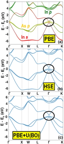
Within density functional theory (DFT) approximate exchange-correlation functionals are used to describe the many-body interactions between electrons. Semi-local functionals, such as the generalized gradient approximation (GGA) of Perdew, Burke, and Ernzerhof (PBE) only contain a dependence on the local density and its gradient. Therefore, they are computationally efficient. However, these functionals fail to describe correctly the electronic properties of some materials, owing to the self-interaction error (SIE), the spurious electrostatic interaction of an electron with itself. For example, for the semiconductor InAs, one of the key materials currently considered for quantum computing applications, the PBE functional produces no band gap, as shown below. The effect of SIE may be mitigated by using hybrid functionals, which contain a fraction of exact (Fock) exchange, such as the Heyd-Scuseria-Ernzerhof (HSE) functional, as shown below for InAs. However, owing to the non-locality of the exact exchange, the computational cost of hybrid functionals is too high for simulations of e.g., large interface models with hundreds of atoms. The DFT+U approach offers a balance between accuracy and efficiency by adding a Hubbard U correction to certain orbitals. The value of U is a parameter, which is often determined by fitting to experiments. We have developed a new method of machine learning the Hubbard U parameter by Bayesian optimization (BO). The objective function is formulated to find the value(s) of U that reproduce as closely as possible the band structure obtained from a hybrid functional. DFT+U(BO) produces band structures of comparable quality to hybrid functionals at the computational cost of a semi-local functional, as shown below for InAs. This enables performing unprecedented simulations of interfaces between materials that could not be described reliably with semi-local functionals.
npj Computational Materials 6, 180 (2020)
Structure Prediction of Epitaxial Inorganic Interfaces with Ogre
Inorganic interfaces lie at the heart of semiconductor, spintronic, and quantum devices. The device functionality and performance often hinge on the electronic and magnetic properties of the interface, as well as on its quality. As devices become increasingly smaller precise control over interface structure becomes increasingly critical. At the same time, the configuration space of possible inorganic interfaces is vast and largely unexplored, owing to the almost infinite number of ways different materials can be combined to form interfaces. The experiments required to fabricate high-quality defect-free interfaces and devices are costly and time consuming. Therefore, it is unfeasible to explore the space of possible structures and compositions by experimental means alone. Computer simulations may significantly accelerate the discovery and design of new inorganic interfaces with desirable properties for semiconductor, spintronic, and quantum devices.
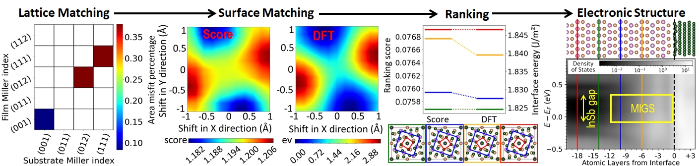
We have implemented in Ogre the capability to perform structure prediction of epitaxial inorganic interfaces by lattice and surface matching. Here, an example is shown for an interface of Fe on top of InSb. In the lattice matching step a scan over combinations of substrate and film Miller indices is performed to identify the domain-matched interfaces with the lowest mismatch, where commensurability is achieved with different integer multiple of the substrate and film unit cells. Subsequently, surface matching is conducted by Bayesian optimization to find the optimal interfacial distance and in-plane registry between the substrate and film. For the objective function, we have formulated a geometric score function, based on the overlap and empty space between atomic spheres at the interface. The score function reproduces the results of density functional theory (DFT) at a fraction of the computational cost. The optimized interfaces are pre-ranked using a score function based on the similarity of the atomic environment at the interface to the bulk environment. Final ranking of the top candidate structures is performed with DFT. Then, the electronic and magnetic properties of the most stable interface structure(s) may be studied. Here, a plot of the density of states (DOS) as a function of position across the interface shows metal induced gap states (MIGS) penetrating from the Fe into the InSb and gradually decaying over several layers.
J. Chem. Phys., 155, 034111 (2021); J. Phys. Condensed Matter, 34, 233002 (2022)
CdTe as a Prospective Tunnel Barrier at the InSb/α-Sn Interface
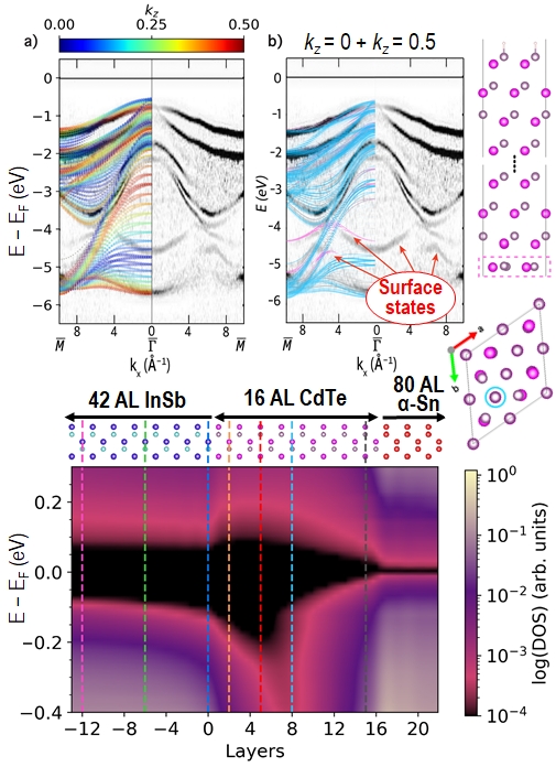
In devices aiming to produce Majorana zero modes, it is desirable to fine-tune the coupling at an interface between a semiconductor nanowire and a superconductor. To this end, we propose inserting a wide-gap tunnel barrier at the interface and carefully controlling its thickness to achieve the desired coupling strength. We used DFT simulations to assess CdTe as a prospective tunnel barrier at the InSb/α-Sn interface. Our DFT+U(BO) method enabled very large simulations of an interface with 42 atomic layers (AL) of InSb, 80 AL of α-Sn, and up to 16 AL of CdTe.
To validate our results we compared the calculated band structure of CdTe to angle-resolved photoemission spectroscopy (ARPES) experiments. Our “z-unfolding” method enabled us to correctly reproduce the contributions from kz values of 0 and 0.5 and the signatures of the 2×2 surface reconstruction seen in the ARPES experiment. Z-unfolding projects the band structure of a supercell slab model onto the appropriate unit cell in real space that corresponds to a surface Brillouin zone with a finite thickness in k-space.
We then show how varying the thickness of the CdTe tunnel barrier affects the electronic properties of the α-Sn/InSb interface, including the penetration depth of metal-induced gap states (MIGS) from the α-Sn into the InSb and the band alignment between the three materials. We also reveal the interplay between the quantum size effect, the MIGS from the α-Sn, and states penetrating from the InSb in the evolution of the band gap across the CdTe tunnel barrier. Our results indicate the relevant tunnel barrier thickness range that would be of interest to test experimentally.
ACS Applied Materials & Interfaces 15, 16288 (2023)
Electronic structure of InAs and InSb surfaces
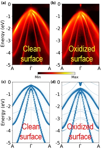
Superconductor/ semiconductor interfaces are among the leading materials platforms for the realization of Majorana-based quantum computing schemes. The superconductor is often grown epitaxially on top of the narrow-gap semiconductors InAs and InSb, which possess high spin-orbit coupling. It is important to understand the electronic structure of InAs and InSb surfaces because it plays a key role in the properties of quantum devices. We have studied the electronic structure of InAs(001), InAs(111), and InSb(110) surfaces using a combination of density functional theory (DFT) and angle-resolved photoemission spectroscopy (ARPES). DFT simulations of large surface models are enabled by the DFT+U(BO) method we have developed. To facilitate direct comparison with ARPES results, we have implemented a “bulk unfolding” scheme by projecting the calculated band structure of a supercell surface slab model onto the bulk primitive cell. The band structures obtained from DFT+U(BO) are overall in excellent agreement with ARPES experiments. The combination of theory and experiment has enabled us to elucidate the effects of surface reconstructions on the electronic structure of the InAs(001) surface and the effect of oxidation on the electronic structure of the InAs(111) and InSb(110) surfaces. For InAs(111), shown here, oxidation leads to significant band bending and produces an electron pocket. This is attributed to charge transfer from the surface In atom to the adsorbed O atom. In addition, we have used DFT simulations in conjunction with scanning tunneling microscopy (STM) and scanning tunneling spectroscopy (STS) to elucidate the electronic structure of defects on the InAs(111) surface.
Advanced Quantum Technologies, 5, 2100033 (2022); Cryst. Growth Des. 22, 5958 (2022)
Topological Interfaces
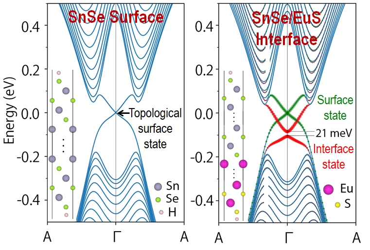
SnSe in a topological crystalline insulator (TCI), a material that is insulating in the bulk but has a conducting state at the surface, which is topologically protected by time reversal symmetry and the crystal symmetry. We conducted DFT simulations of an epitaxial interface between SnSe and the ferromagnetic insulator (FMI), EuS. The magnetic proximity effect breaks the time reversal symmetry and opens a gap of 21 meV in the topological interface state of SnSe, shown in red. Because the magnetic proximity effect is short ranged and confined to the interface, the topological state at the top surface of SnSe, shown in green, in unperturbed. Charge transfer at the interface leads to band bending and shifts the gapped interface states below the Fermi level by 88 meV. The topological interface state of SnSe/EuS (111) has a larger gap and a smaller binding energy than e.g., Bi2Se3/EuS. Hence, it could be a potential candidate for implementing quantum/ topological devices.
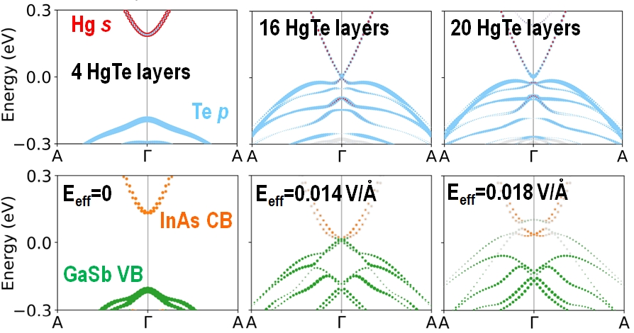
A 2D topological insulator (2DTI) phase can emerge at an epitaxial interface between two materials that are not inherently topological insulators. HgTe is a semi-metal with an inverted band structure and CdTe is a wide-gap semiconductor. When HgTe is grown on top of CdTe, with 4 layers, owing to the quantum size effect, the HgTe film is a trivial insulator. At a critical thickness of 16 layers (5.1 nm) of HgTe band crossing occurs and subsequently an inverted gap opens. Both InAs and GaSb are semiconductors. If an electric field is applied across the InAs/GaSb interface band crossing can be achieved between the InAs conduction band and the GaSb valence band. If the electric field is increased further, an inverted gap can be opened.
Magnetic Interfaces
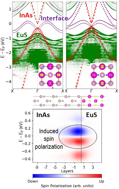
Spintronic devices harness the electron’s spin as well as its electric charge to encode information. At an interface between a semiconductor and a magnetic material, proximity-induced magnetization can produce spin polarization in the semiconductor. We studied the interface between the ferromagnetic insulator EuS and the semiconductor InAs. In agreement with ARPES experiments, we find that the EuS valence band maximum (VBM), colored in green, lies below the InAs VBM, colored in red. In addition, dispersed interface states, colored in purple, emerge at the top of the InAs VBM. These states, which do not exist in either material separately, are contributed mainly by the InAs layer adjacent to the interface. They are localized at the interface and may be attributed to charge transfer from the EuS to the InAs. The interface bonding configuration, with the structure on the left predicted to be the most stable, affects the position of the EuS VBM with respect to the InAs VBM, as well as the dispersion of the interface states. Proximity-induced spin polarization appears in the InAs in the vicinity of the interface, in the same region where the interface states appear.
We have also investigated interfaces of the magnetic Heusler compounds Ni2MnIn and Ti2MnIn with the III-V semiconductors InAs and InSb, respectively. We find that the magnetic interactions at the interface are weak and local in space and energy. The decisive factor for the induced spin polarization around the Fermi level of the semiconductor is the spin polarization around the Fermi level in the Heusler, rather than the overall magnetic moment. As a result, the ferrimagnetic narrow-gap semiconductor Ti2MnIn induces a more significant spin polarization in the InSb than the ferromagnetic metal Ni2MnIn induces in the InAs. This is explained by the position of the Heusler’s transition metal d states with respect to the Fermi level.
Phys. Rev. Mater. 5, 064606 (2021); Phys. Rev. Materials, 7, 026203 (2023)